Analyzing the electronic states of a heavily
overdoped high temperature superconductor
SUMMARY
Superconductors are materials in which some of the electrons are
able to lose their individual identity by pairing up and 'condensing'
into a single macroscopic quantum mechanical state. This produces
exotic and useful properties including the ability to conduct electrical
current with zero resistance. Some common materials are superconductors
at very low temperatures (e.g. lead at 7K, mercury at 4K, aluminum
at 1K), and in these materials the pairing mechanism is well understood.
However, in the mid-1980s, a new class of multi-layered copper-based
superconductors was discovered with transition temperatures ranging
above 100K (-173°C, which counts as "high temperature"
in this field). These posed two of the most important unsolved questions
in physics: what makes these materials superconductors, and is it
possible to achieve superconductivity at room temperature?
|

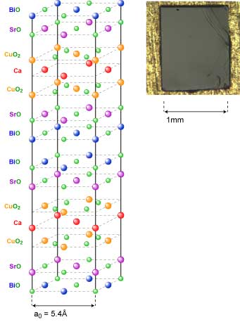
Figure 1: The Bi2Sr2CaCu2O8+x unit cell, and a photograph
of the heavily overdoped sample used in the Davis Group study.
|
|
One of the most widely studied high temperature superconductors
is Bi2Sr2CaCu2O8+x
(Bi-2212, figure 1). Like the rest of its family, the superconductor
is produced by doping its insulating parent compound with
a certain quantity of excess charge carriers (in this case,
by adding more oxygen). To understand what makes these materials
work, it is necessary to understand how the doping produces
the superconductivity, and why it disappears when the materials
are doped too much. One path is to study crystals that are
heavily overdoped yet still superconducting, to see what states
begin to evolve, and to test various competing theoretical
predictions about what should happen.
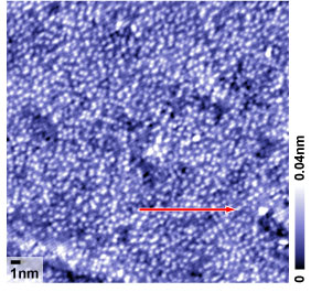
Using a purpose-built scanning tunneling microscope (STM)
in the ultra-low vibration research laboratory of the Davis
Group at Cornell University, graduate student James Slezak
produced a topograph (figure 2) of the surface of the crystal,
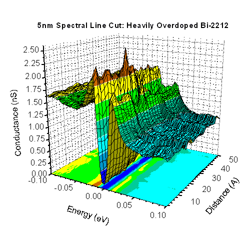
and a spectroscopic line cut of the density of states (figure
3). The shape and features of this 3D surface provides important
information about the electronic state of the material and
its spatial evolution.
|
|

Figure 2 : Atomic resolution topographic image of the heavily
overdoped superconductor Bi-2212, with red line indicating
position and direction of spectroscopic line-cut.
|
|

Figure 3: A line cut representing the density of electronic
states in the superconductor along the line indicated in figure
2.
|
ANALYSIS IN ORIGIN
The line cut data were imported from the STM control software using
Origin's ASCII data Import Wizard. There was one spectrum for each
point along the line, and these were combined onto one worksheet
using the copy and paste functions. Each spectrum gives the tunneling
conductance of the STM tip-sample junction as a function of the
bias voltage, which is conventionally interpreted as the density
of states of the material as a function of energy.
|
The horizontal axis of the worksheet corresponded to distance
along the line cut, so the top row of the worksheet contained
the position, in nanometers, of each spectrum in the column
below. To produce the 3D graph, the worksheet was converted
to a matrix (using Origin's direct conversion method). To
reduce the number of points plotted, the size of the matrix
along each axis was halved using the "shrink matrix"
command and smoothed. The graph was produced as a 3D color
map surface plot.
ACKNOWLEDGMENTS
|
|
 |
This research was conducted at the J.
C. Davis Group, Laboratory of Atomic and Solid State Physics,
at Cornell University. The samples were prepared by Kazuhiro Fujita
(U. Tokyo), Dr. Hiroshi Eisaki (AIST-Tokyo) and Prof. Shin-ichi
Uchida (U. Tokyo) in Japan, and were overdoped at the Davis Group
labs at Cornell by Kazuhiro Fujita and James Slezak. The STM experiment
was performed by James Slezak, Kazuhiro Fujita, Dr. Jinho Lee (Cornell)
and Alfred Wang (Cornell).
James Slezak
is a Ph.D. student in the Department of Physics at Cornell University.